12th class Physics unit 7 MCQs
chapter 7 MCQs 12th Class physics
Electronics:
1. A diode characteristic curve is a plot between:
a. Voltage and current
b. Current and time
c. Forward voltage and reverse voltage
d. Voltage and time
2. The colour of light emitted by a LED depends on:
a. The amount of forward current
b. Its forward bias
c. The types of semiconductor material used
d. Its reverse bias
3. In a half-wave rectifier the diode conducts during:
a. A portion of the negative half of the input cycle
b. Both halves of the input cycle
c. One half of the input cycle
d. A portion of the positive half of the input cycle
4. In a bridge rectifier of figure when V is positive at point B with respect to point A, which diodes are ON?
a. D2 and D3
b. D2 and D4
c. D1 and D4
d. D1 and D4
5. The common emitter current amplification factor is given by:
a. lE/lB
b. lc/lE
c. lB/lE
d. lc/lB
6. Truth table of logic function:
a. Display all its input/output possibilities
b. Summarizes its output values
c. Is not based on logic algebra
d. Tabulates all its input conditions only
7. The output of a two inputs OR gate is 0 only when its:
a. Both inputs are 1
b. Both inputs are 0
c. Either input is 0
d. Either input is 1
8. A two inputs NAND gate with inputs A and B has an output 0 if:
a. A is 0
b. B is 0
c. Both A and B are zero
d. Both A and B are 1
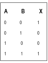
9. The truth table shown below is for

a. AND gate
b. XNOR gate
c. NAND gate
d. OR gate
10. Voltage gain of the common emitter npn-transister as an amplifier is:
a. β Vc/Rc
b. βrIc / Rc
c. βRc/ rIc
d. β lc/Rc
11. Potential difference across depletion region in ease of silicon:
a. 0.8 V
b. 0.6 V
c. 0.9 V
d. 0.7 V
12. The potential barriers for germanium at room temperature is:
a. 0.7 V
b. 0.3 V
c. 0.9 V
d. 0.5 V
13. A transistor has β= 100 and Lc= 10mA Its value of lB= ?
a. 0.01 µA
b. 1 µA
c. 100 µA
d. 0.1 µA
14. Transistor was discovered by:
a. John Bardeen
b. Young
c. Shale’s
d. I. Curie
15. Reverse current flows due to:
a. Electrons
b. Majority charge carriers
c. Holes
d. Minority charge carriers
16. When a PN-junction is reverse biased the depletion region is:
a. Normal
b. Widened
c. Narrowed
d. None of these
17. Transistors are made from:
a. Insulator
b. Plastics
c. Doped semi conductors
d. Metals
18. The central region of a transistor is called:
a. Collector
b. Base
c. Neutral
d. Emitter
19. Which factor does not affect the conductivity of Pn-junction diode?
a. Voltage
b. Doping
c. Pressure
d. Temperature
20. An expression for current gain of a transistor is given by:
a. β= lC – lB
b. β= lB / lC
c. β= lC / lB
d. β= lB + lC
21. A pn-junction cannot be used as:
a. Detector
b. Rectifier
c. LED
d. Amplifier
22. The ratio of potential barriers of Ge to Si at room temperature is:
a. 2:5
b. 7:3
c. 3:7
d. 1:3
23. A sensor of light is:
a. Diode
b. Transistor
c. Light dependent Resistance
d. LED
24. A device which converts low voltage or current to high voltage or current is called:
a. Rectifier
b. Transformer
c. Amplifier
d. AC-generator
25. Depletion region carries:
a. Ions
b. -ve charge
c. No charge
d. +ve charge
